- 您现在的位置:买卖IC网 > Sheet目录3882 > PIC24F08KL301-I/SS (Microchip Technology)IC MCU 16BIT 8KB FLASH 20-SSOP
CHAPTER 4 PORT FUNCTIONS
User’s Manual U15905EJ2V1UD
142
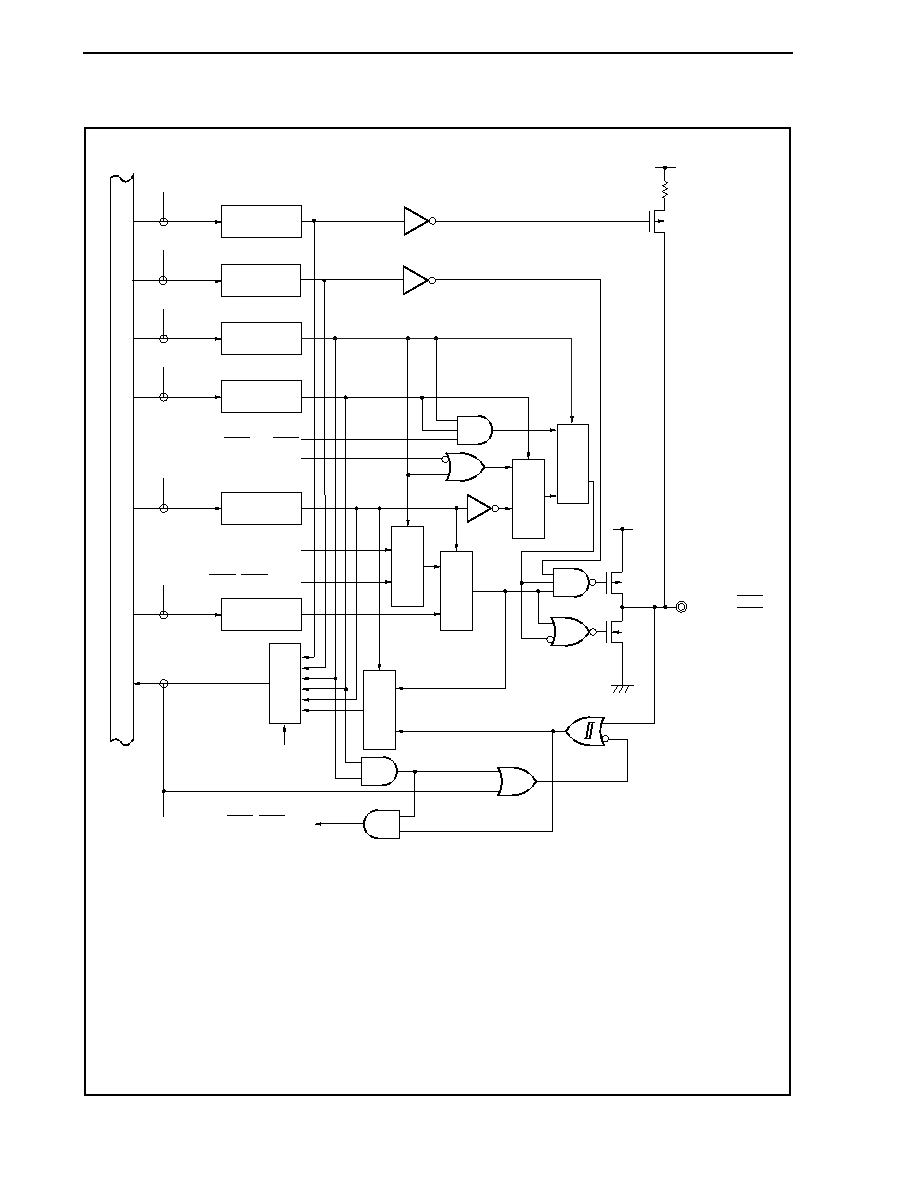
Figure 4-23. Block Diagram of P912 and P915
Internal
bus
WRPMC
RD
Address
SCK2, SCK3 output
A12, A15 output
SCK2, SCK3 input
WRPORT
P912/A12/SCK2,
P915/A15/SCK3
PMC9n
WRPFC
PFC9n
Selector
Output enable signal of
SCK2 and SCK3
Output buffer off signal
Selector
WRPU
PU9n
WRPM
PM9n
Output latch
(P9n)
WRPF
PF9n
PMC9
PFC9
PU9
PM9
P9
PF9
EVDD
P-ch
EVDD
EVSS
P-ch
N-ch
Selector
Caution
These pins do not have hysteresis characteristics in the port mode.
They have hysteresis characteristics only when an input-pin alternate function is used.
Remarks 1. P9:
Port register 9
PM9:
Port mode register 9
PMC9: Port mode control register 9
PFC9: Port function control register 9
PF9:
Port function register 9
PU9:
Pull-up resistor option register 9
Output buffer off signal: Signal that is active in the IDLE/STOP mode or during bus hold
2. n = 12 or 15
发布紧急采购,3分钟左右您将得到回复。
相关PDF资料
PIC18LF1220T-I/ML
IC MCU FLASH 2KX16 EEPROM 28QFN
PIC18LF1220T-I/SO
IC MCU FLASH 2KX16 EEPROM 18SOIC
PIC16F716-I/SS
IC PIC MCU FLASH 2KX14 20SSOP
PIC18F1320T-E/ML
IC MCU FLASH 4KX16 EEPROM 28QFN
PIC16LF87T-I/ML
IC MCU FLASH 4KX14 EEPROM 28QFN
PIC18F25J10-I/SS
IC PIC MCU FLASH 16KX16 28SSOP
PIC16F88T-E/SS
IC MCU FLASH 4KX14 EEPROM 20SSOP
PIC16C621A-04/SO
IC MCU OTP 1KX14 COMP 18SOIC
相关代理商/技术参数
PIC24F08KL301T-I/MQ
功能描述:16位微控制器 - MCU 8KB FLASH 1KB RAM 512B 3V 10-BIT ADC RoHS:否 制造商:Texas Instruments 核心:RISC 处理器系列:MSP430FR572x 数据总线宽度:16 bit 最大时钟频率:24 MHz 程序存储器大小:8 KB 数据 RAM 大小:1 KB 片上 ADC:Yes 工作电源电压:2 V to 3.6 V 工作温度范围:- 40 C to + 85 C 封装 / 箱体:VQFN-40 安装风格:SMD/SMT
PIC24F08KL301T-I/SO
功能描述:16位微控制器 - MCU 8KB FLASH 1KB RAM 512B 3V 10-BIT ADC RoHS:否 制造商:Texas Instruments 核心:RISC 处理器系列:MSP430FR572x 数据总线宽度:16 bit 最大时钟频率:24 MHz 程序存储器大小:8 KB 数据 RAM 大小:1 KB 片上 ADC:Yes 工作电源电压:2 V to 3.6 V 工作温度范围:- 40 C to + 85 C 封装 / 箱体:VQFN-40 安装风格:SMD/SMT
PIC24F08KL301T-I/SS
功能描述:16位微控制器 - MCU 8KB FLASH 1KB RAM 512B 3V 10-BIT ADC RoHS:否 制造商:Texas Instruments 核心:RISC 处理器系列:MSP430FR572x 数据总线宽度:16 bit 最大时钟频率:24 MHz 程序存储器大小:8 KB 数据 RAM 大小:1 KB 片上 ADC:Yes 工作电源电压:2 V to 3.6 V 工作温度范围:- 40 C to + 85 C 封装 / 箱体:VQFN-40 安装风格:SMD/SMT
PIC24F08KL302
制造商:MICROCHIP 制造商全称:Microchip Technology 功能描述:Low-Power, Low-Cost, General Purpose 16-Bit Flash Microcontrollers with nanoWatt XLP Technology
PIC24F08KL302-I/ML
功能描述:16位微控制器 - MCU 8KB FLASH 1KB RAM 256B 3V RoHS:否 制造商:Texas Instruments 核心:RISC 处理器系列:MSP430FR572x 数据总线宽度:16 bit 最大时钟频率:24 MHz 程序存储器大小:8 KB 数据 RAM 大小:1 KB 片上 ADC:Yes 工作电源电压:2 V to 3.6 V 工作温度范围:- 40 C to + 85 C 封装 / 箱体:VQFN-40 安装风格:SMD/SMT
PIC24F08KL302-I/MQ
功能描述:16位微控制器 - MCU 8KB FL 1KB RAM 256B 3V RoHS:否 制造商:Texas Instruments 核心:RISC 处理器系列:MSP430FR572x 数据总线宽度:16 bit 最大时钟频率:24 MHz 程序存储器大小:8 KB 数据 RAM 大小:1 KB 片上 ADC:Yes 工作电源电压:2 V to 3.6 V 工作温度范围:- 40 C to + 85 C 封装 / 箱体:VQFN-40 安装风格:SMD/SMT
PIC24F08KL302-I/SO
功能描述:16位微控制器 - MCU 8KB FLASH 1KB RAM 256B 3V RoHS:否 制造商:Texas Instruments 核心:RISC 处理器系列:MSP430FR572x 数据总线宽度:16 bit 最大时钟频率:24 MHz 程序存储器大小:8 KB 数据 RAM 大小:1 KB 片上 ADC:Yes 工作电源电压:2 V to 3.6 V 工作温度范围:- 40 C to + 85 C 封装 / 箱体:VQFN-40 安装风格:SMD/SMT
PIC24F08KL302-I/SP
功能描述:16位微控制器 - MCU 8KB FLASH 1KB RAM 256B 3V RoHS:否 制造商:Texas Instruments 核心:RISC 处理器系列:MSP430FR572x 数据总线宽度:16 bit 最大时钟频率:24 MHz 程序存储器大小:8 KB 数据 RAM 大小:1 KB 片上 ADC:Yes 工作电源电压:2 V to 3.6 V 工作温度范围:- 40 C to + 85 C 封装 / 箱体:VQFN-40 安装风格:SMD/SMT